
Applied Materials Inc. and Arizona State University (ASU) have officially opened a $270 million advanced semiconductor research and development facility in Arizona's East Valley. The new Materials-to-Fab Center is designed to accelerate innovation in chip technology and strengthen the region's position as a critical hub for the U.S. semiconductor industry.
Key Takeaways
- Applied Materials and ASU have partnered to launch a $270 million semiconductor research facility.
- The center, located at ASU Research Park, includes 50,000 square feet of cleanroom space.
- Its primary goal is to fast-track chip innovations from concept to prototype, focusing on AI and high-performance computing.
- The collaboration aims to train a new generation of engineers and researchers for the semiconductor industry.
A Major Investment in U.S. Semiconductor Innovation
On Thursday, October 12, 2025, Applied Materials and Arizona State University unveiled their joint venture, the Materials-to-Fab Center. This state-of-the-art facility represents a significant investment aimed at bolstering the domestic semiconductor ecosystem. The center is strategically located within the university’s MacroTechnology Works building at ASU Research Park, placing it at the heart of a growing technology corridor.
The collaboration brings together Applied Materials, a global leader in materials engineering solutions for the semiconductor industry, and ASU, a top-tier research university. The partnership leverages the strengths of both institutions: Applied Materials provides industry-leading manufacturing equipment and expertise, while ASU contributes its extensive research capabilities and engineering talent. The facility is intended to serve as a collaborative space for academia, researchers, and other industry partners to work together on next-generation chip technologies.
Why This Matters for the U.S.
The semiconductor industry is critical for national security and economic competitiveness. Recent global supply chain disruptions have highlighted the need for the United States to increase its domestic chip manufacturing and research capabilities. Initiatives like the Materials-to-Fab Center are central to this effort, aiming to reduce reliance on foreign manufacturing and secure U.S. leadership in key technological areas like artificial intelligence.
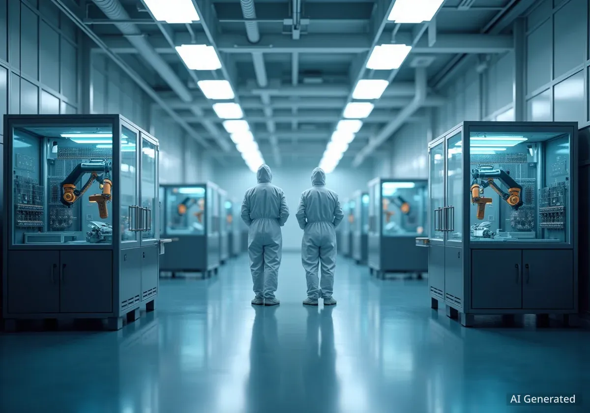
Inside the State-of-the-Art Facility
The Materials-to-Fab Center is a substantial facility, spanning a total of 70,000 square feet. The design prioritizes the specialized environments required for advanced semiconductor research and prototyping.
The core of the center is its 50,000-square-foot cleanroom. This highly controlled environment is essential for fabricating and testing sensitive semiconductor components, where even microscopic dust particles can ruin a prototype. In addition to the cleanroom, the facility includes 20,000 square feet of dedicated wet and dry labs. These labs are equipped with specialized tools for materials analysis, chemical processing, and other critical research functions.
By housing Applied Materials' advanced semiconductor manufacturing equipment on-site, the center creates a unique environment. It allows researchers and students to move seamlessly from theoretical ideation to hands-on prototyping, a process that can significantly shorten development cycles for new technologies.
Facility at a Glance
- Total Investment: $270 million
- Total Area: 70,000 square feet
- Cleanroom Space: 50,000 square feet
- Lab Space: 20,000 square feet
- Location: ASU Research Park, Tempe, Arizona
Fueling the Future of AI and High-Performance Computing
The primary mission of the Materials-to-Fab Center is to accelerate the development of new chip technologies that are crucial for future advancements in artificial intelligence (AI) and high-performance computing. These fields demand increasingly powerful and efficient processors, and the center is positioned to be a key incubator for such innovations.
During the ribbon-cutting ceremony, Dr. Prabu Raja, president of Applied Materials’ semiconductor products group, emphasized the strategic importance of the collaboration.
“Our collaboration will also help to create a new generation of talent to feed this ecosystem. These students are already working with Applied Materials’ equipment.”
Dr. Raja noted that the partnership is already yielding tangible results, even in its early stages. He projected that the work conducted at the center is on track to produce more than 30 research publications and eight patents. “The Materials-to-Fab Center has already accomplished a lot and we are just getting started,” he added.
Developing a Skilled Workforce for a Growing Industry
Beyond technological innovation, a central goal of the new facility is workforce development. The semiconductor industry faces a significant talent shortage, and this partnership directly addresses that challenge by providing students with invaluable hands-on experience.
By working with the same advanced equipment used in commercial fabrication plants, ASU engineering students will graduate with practical skills that are in high demand. This direct exposure to industry-standard tools and processes makes them better prepared to contribute to the workforce immediately upon graduation.
The center creates a pipeline of talent that will support not only Applied Materials but also the broader semiconductor ecosystem in Arizona and across the United States. This focus on training the next generation of engineers and researchers is seen as a critical component for ensuring the long-term success and sustainability of the domestic chip industry.